XII. CAUSES OF NOISE PROPERTIES IN A SIGNAL SOURCE
12.1 Power-law Noise Processes
Section IX pointed out the five commonly used power-law models of noise. With respect to Sf (f), one can estimate a straight line slope (on a log-log scale) which corresponds to a particular noise type. This is shown in figure 12.1 (also fig.9.1).
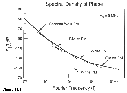
We can make the following general remarks about power-law noise processes:
1.Random walk FM (1/f4) noise is difficult to measure since it is usually very close to the carrier. Random walk FM usually relates to the OSCILLATOR'S PHYSICAL ENVIRONMENT. If random walk FM is a predominant feature of the spectral density plot then MECHANICAL SHOCK, VIBRATION, TEMPERATURE, or other environmental effects may be causing "random" shifts in the carrier frequency.
2.Flicker FM (1/f3) is a noise whose physical cause is usually not fully understood but may typically be related to the PHYSICAL RESONANCE MECHANISM OF AN ACTIVE OSCILLATOR or the DESIGN OR CHOICE OF PARTS USED FOR THE ELECTRONICS, or ENVIRONMENTAL PROPERTIES. Flicker FM is common in high-quality oscillators, but may be masked by white FM (1/f2) or flicker PM (1/f) in lower-quality oscillators.
3.White FM (1/f2) noise is a common type found in PASSIVE-RESONATOR FREQUENCY STANDARDS. These contain a slave oscillator, often quartz, which is locked to a resonance feature of another device which behaves much like a high-Q filter. Cesium and rubidium standards have white FM noise characteristics.
4.Flicker PM (1/f) noise may relate to a physical resonance mechanism in an oscillator, but it usually is added by NOISY ELECTRONICS. This type of noise is common, even in the highest quality oscillators, because in order to bring the signal amplitude up to a usable level, amplifiers are used after the signal source. Flicker PM noise may be introduced in these stages. It may also be introduced in a frequency multiplier. Flicker PM can be reduced with good low-noise amplifier design (e.g., using rf negative feedback) and hand-selecting transistors and other electronic components.
5.White PM (f0) noise is broadband phase noise and has little to do with the resonance mechanism. It is probably produced by similar phenomena as flicker PM (1/f) noise. STAGES OF AMPLIFICATION are usually responsible for white PM noise. This noise can be kept at a very low value with good amplifier design, hand-selected components, the addition of narrowband filtering at the output, or increasing, if feasible, the power of the primary frequency source.13
12.2 Other types of noise
A commonly encountered type of noise from a signal source or measurement apparatus is the presence of 60 Hz A.C. line noise. Shown in figure 12.2 is a constant white PM noise source with 60 Hz, 120 Hz and 180 Hz components added. This kind of noise is usually caused by AC power getting into the measurement system or the source under test. In the plot of Sf (f), one observes discrete line spectra. Although Sf (f) is a measure of spectral density, one can interpret the line spectra with no loss of generality, although one usually does not refer to spectral densities when characterizing discrete lines. Figure 12.3 is the time domain representation of the same white phase modulation level with 60 Hz noise. Note that the amplitude of s y(t) varies up and down depending on sampling time. This is because in the time domain the sensitivity to a periodic wave varies directly as the sampling interval. This effect (which is an alias effect) is a very powerful tool for filtering out a periodic wave imposed on a signal source. By sampling in the time domain at integer periods, one is virtually insensitive to the periodic (discrete line) term.
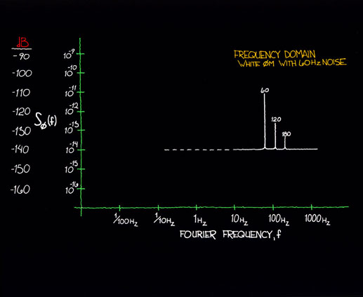
Figure 12.2: 60 Hz and harmonics are easily distinguished in a phase-noise measurement.
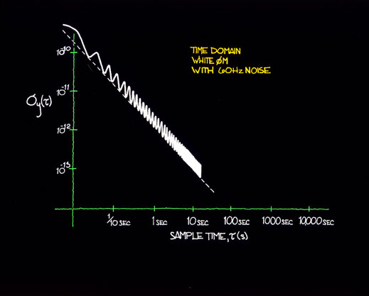
Figure 12.3: It is not easy to interpret an Allan deviation plot when 60 Hz noise is present on an oscillating signal.
For example, diurnal variations in data due to day to day temperature, pressure, and other environmental effects can be eliminated by sampling the data once per day. This approach is useful for data with only one periodic term.
Figure 12.4 shows the kind of plot one might see of Sf (f) with vibration and acoustic sensitivity in the signal source with the device under vibration. Figure 12.5 shows the translation to the time domain of this effect. Also noted in figure 12.4 is a (typical) flicker FM behavior in the low frequency region. In the translation to time domain (fig. 12.5), the flicker FM behavior masks the white PM (with the superimposed vibration characteristic) for long averaging times.
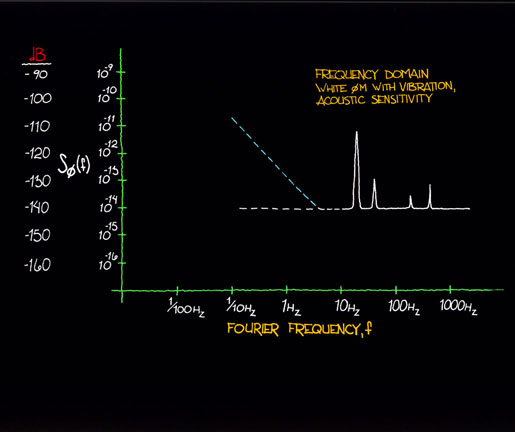
Figure 12.4: An oscillator under vibration causes sideband noise modulation that is apparent in a phase-noise measurement.
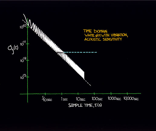
Figure 12.5: The Allan deviation of an oscillator under vibration causes a general increase in the level of frequency instability.
Figure 12.6 shows examples of plots of two power law processes (Sf (f)) with a change in the flicker FM level. (Example 1 is identical to the example given in sec. XI.) Figure 12.7 indicates the effect of a lower flicker FM level as translated to the time domain. Note again the existence of both power law noise processes. However for a given averaging time (or Fourier frequency) one noise process may dominate over the other.
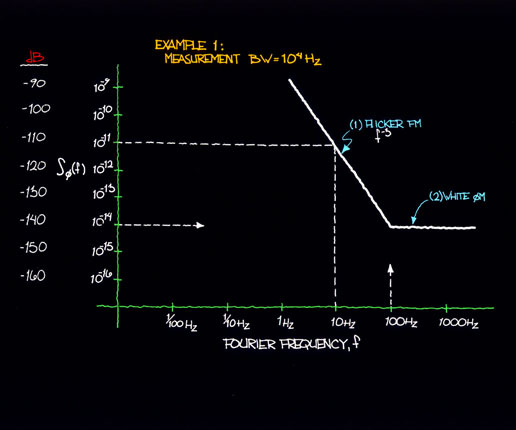
Figure 12.6a
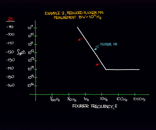
Figure 12.6b
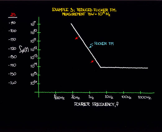
Figure 12.6c
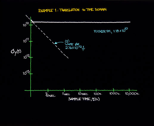
Figure 12.7a
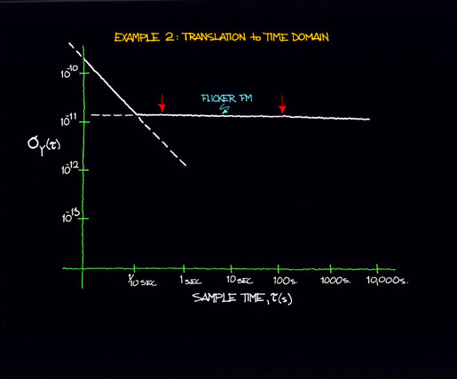
Figure 12.7b
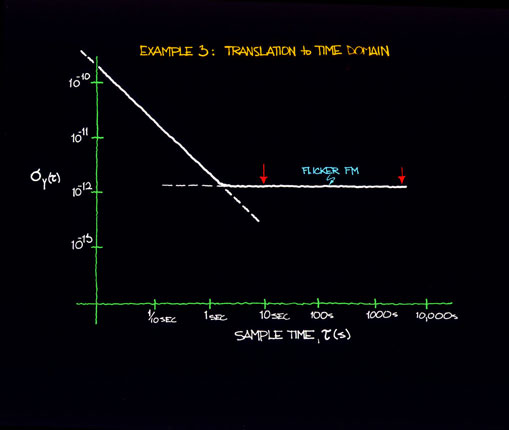
Figure 12.7c
Excess device noise from transistors, capacitors, resistors, and the like can introduce a low frequency noise which has been referred to as "popcorn" noise because of its sonic qualities. Figure 12.8 shows a plot of Sf (f) from a signal source having such excess low frequency noise. Figure 12.9 is the time domain representation. The rise in amplitude of s y for long averaging times is particularly aggravating. The solution to this kind of problem if it is introduced by devices is to carefully grade the devices in the assembly and testing process.
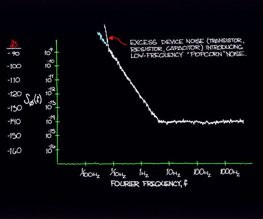
Figure 12.8
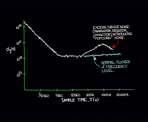
Figure 12.8
Stages of amplification following a signal source many times rely on local degenerate or overall negative feedback schemes in order to minimize the excess noise from active gain elements (such as op-amps and transistors). This is the recommended design approach. However, phase shift in the negative feedback circuit or poor bandwidth in the gain elements can result in poor high frequency noise behavior. Figure 12.10 shows a kind of result one might see as a gradual rise in Sf (f) because of insufficient negative feedback at high Fourier frequencies.
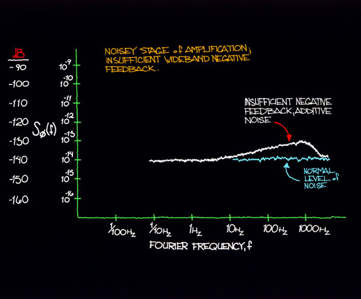
Figure 12.10
Section X discusses aliasing in the frequency domain. Figure 12.11 shows the resultant measurement anomaly due to digital sampling of a poorly bandlimited (anti-aliased) white noise source. Noise voltage above the sampling frequency fs is folded into the analysis region of interest. Note also that the stopband ripple characteristics are folded into the high-frequency portion of the passband. For a given sampling frequency, a compromise exists between increasing the high-frequency extent of the analysis band and improving the anti-aliasing filter's stopband rejection. Section X has an example of the filter requirements for a particular case.
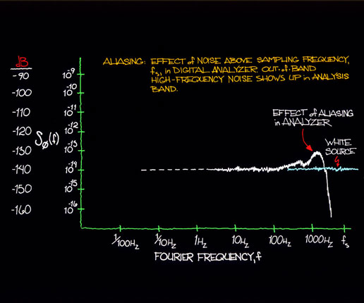
Figure 12.11
Main Page Table of Contents
Go to section:
Summary and Introduction
I
II
III
IV
V
VI
VII
VIII
IX
X
XI
XII
Conclusion
References