


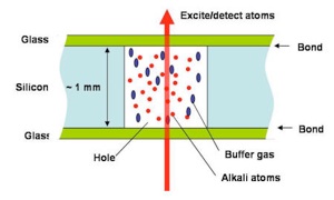
The basic concept of the cell design is shown in the figure below. The cell is formed in a wafer of Si with glass wafers bonded to both sides. A hole, etched or drilled in the Si wafer, forms a cavity in which the alkali atoms, along with an appropriate buffer gas, reside. The glass wafer windows confine the atoms inside the cell and allow access for optical fields, which prepare, excite and detect the atomic oscillation. The use of Si to form the cavity allows for highly scalable fabrication using photolithographically defined geometries: cell sizes ranging from several millimeters to tens of micrometers should be feasible. In addition, the use of machining technologies commonly used in microelectromechanical systems (MEMS), and nanotechnology permits the fabrication of many closely-spaced cells simultaneously on a single wafer. Finally, the planar structure makes integration with other components faster and more reliable than it is with conventional cell structures.
Overall microfabricated cell design. The cell is formed by
a hole etched in a Si wafer with glass wafers bonded on
the top and bottom.
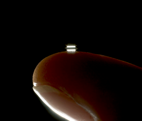
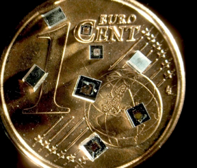
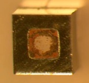
A cell fabricated at NIST containing Cs metal and a buffer gas.
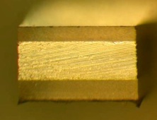
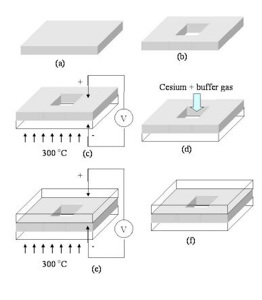
The process used to fabricate the vapor cells is shown in the figure below at left. We start with a Si wafer with a double-sided polish [DSP, (a)] A hole is etched in the wafer (b) using either wet chemical etching or deep reactive-ion etching. A wafer of glass with coefficient of thermal expansion close to that of Si is bonded onto one side of the Si wafer using anodic or field-assisted bonding (c). In this process, the samples are placed in contact and heated to about 300 C. Roughly 1000 V is applied across the samples for several minutes. A strong, hermetic bond is created between the samples. The resulting preform is then placed in an inert environment and alkali atoms are added either by chemical reaction or by direct deposition (d). A second glass wafer is placed on the open side of the preform and bonded to seal the cell (e), after backfilling the enclosure with the appropriate buffer gas. The final sealed cell (f) therefore contains some amount of alkali metal along with a buffer gas. A cell fabricated in this way is shown below.
The microfabrication process for alkali atom vapor cells.
Contact: Svenja Knappe
References:
Photos: Daniel Bayer