


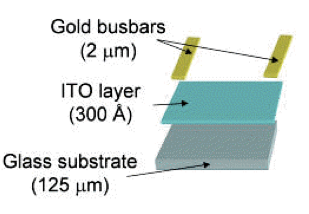
Because of the small size of the microfabricated vapor cells, the number of atoms contained within a cell at room temperature is quite small (typically about 35,000,000 atoms are present). A small number of atoms implies a small amount of light absorbed and a correspondingly small CPT signal. Since the atomic density increases with temperature, the cells are typically operated between 80 °C and 130 °C in order to increase the number of atoms to the point where the absorption is near 50 %. Microfabricated cell heaters are used to heat the cells. These heaters are fabricated by depositing a thin layer of Indium-Tin-Oxide (ITO) onto a glass substrate using electron-beam evaporation. ITO is a transparent, conducting material and therefore can form a resistive heater distributed over the surface of the substrate while still allowing light to pass through. An ITO film of about 30 nm results in a resistance of 100W/sq. Gold busbars deposited near the edges of the final heater elements enable gold wires to be bonded to the component. The other end of the gold wires is attached to the CSAC substrate to provide electrical access.
Critical to the operation of magnetometers is the design of the heater. The magnetic field from any current flowing near the vapor cell will be detected by the atoms, so great care is taken to reduce the effect of the heater currents. To largely cancel the magnetic field produced by the ITO heater current, we configure the current to double back on itself. This is achieved by first laser patterning the ITO so that the current flows through a 120 μm wide strip of ITO (Fig. 2). The meandering path of the current makes the heater resistance high (2 kΩ), reducing the current, and spreads the power dissipation over the majority of the heater, evenly heating the cell window. To create a return path for the current that is separated by only ~10 μm from the path of the input current, we glue two patterned ITO heaters together, the second having the mirror image pattern of the first. Thus, the magnetic field created by the current flowing through the lower ITO layer is canceled by the field of the return current flowing directly above it in the upper ITO layer. To further reduce the effects of the ITO heater currents, we use an alternating current through the heater at a frequency ranging from 2 to 10 kHz. By comparing the measured magnetic field when using alternating and direct currents through the heaters, we observe the field produced by the heaters when using direct current to be 23 nT and the broadening of the magnetic resonance to be 110 Hz (out of a total broadening of 1800 Hz).
We have developed monolithically integrated “in-situ” heaters in the cells as a possible alternative to using ITO heaters. The advantages of this approach over the ITO heaters are:
-
1. These heaters will take up less space if implemented in CSAC – these heaters are fabricated directly inside the cell cavity, so additional chips do not need to be added to the physics package, thus reducing the overall CSAC volume. This is not apparent in this report, since the cells made so far have been larger than those used in the CSAC.
-
2. Possibly lower power – since the heaters are inside the cell cavity and in direct contact with the Cs and the cell’s glass windows (being anodically bonded to the glass), there should be lower thermal resistances since no intermediate barriers exist between the cell and the heater. (Again, this is not immediately apparent from this report since the cells made with heaters so far have had a size and configuration different from those that would be used in the CSAC.)
-
3. The silicon heaters may also be used as temperature sensors. These cells have been fabricated with two coils, one for heating and one for sensing, although so far the sensing function has been only briefly looked at. Alternatively, diodes could be fabricated inside the cells for temperature sensing.
-
4. Monolithic integration – reduces cost of commercialization
The disadvantages compared to the ITO heaters:
-
1. Temperature gradients – the silicon heaters will cause a temperature gradient across the cell window whereas the ITO films (being unpatterned) do not.
-
2. 2. Optical transparency – the ITO heaters are transparent, whereas the silicon heaters are not; thus the silicon heaters would limit the useful area of the cell window.
Fabrication:
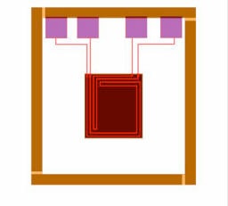
The cells were fabricated using the same general procedure as previous cells – cavities/structures were etched in silicon, bonded to glass to make performs, and the preforms were filled with Cs and N2 buffer gas in the anaerobic chamber and sealed by anodic bonding. The difference is that in addition to simple square cavities, more complex serpentine-shaped structures were etched in silicon using deep reactive ion etching to define the bifilar heater coils. In addition, these heater coils were doped with boron to increase their electrical conductivity. The doped region also extends further out into the chip, outside of the cell cavity, and is patterned into electrical traces and bond pads at the edge of the chip. Metal or epoxy is deposited on the bond pads to enable wirebonding and thus electrical connection to the heater coils. The figure above shows a layout of one such chip.
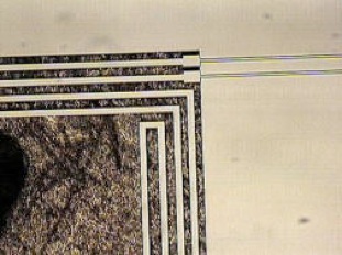
To avoid the dicing process, which could damage the delicate heater coils, open trenches were etched in the wafer to define each chip, with the chips being attached to the wafer by means of thin silicon pieces or “breaktabs” which can be easily broken to remove the chips from the wafer. The figure above right shows one such wafer of cell preforms. The silicon preforms were then filled with Cs from a pipette in the anaerobic chamber, backfilled with 20-25 kPa of N2 buffer gas, and sealed by anodic bonding, where the top glass piece is placed such that the silicon bond pads are exposed.
The figure below shows the fabricated cells. Each cell contains two heater coils, which are 30 mm wide and have the same thickness as the rest of the wafer, thus contacting both the top and bottom glass windows. The resistance of each coil is about a kilohm at room temperature, and remains unchanged before and after anodic bonding despite the high voltages used.
Cesium optical absorption measurements were performed to test the functionality of the heaters. For this, the cells were wire-bonded to a metal chip carrier that had holes drilled in its well to allow light to pass through the cell. (The chip carrier served only to hold the cells and provide the electrical connections to the heaters.) A glass spacer 0.5 mm-thick was placed between the cells and the chip carrier to provide some thermal isolation; nevertheless, the entire chip carrier was heated substantially by the cell heaters (see figure below). The chip carrier leads were connected to a DC power supply, and the power was increased until a clear optical absorption spectrum was obtained, as shown in the figure below. At this point, the temperature of the cell’s outer surface was measured with a thermocouple to be about 75 °C; the heater input power was about 1 watt. The temperatures of the outer surface of the cell’s glass window, the glass spacer, and the chip carrier were then measured using a thermocouple as a function of the heater input power, show in the figure below.
The high heater power consumption is due to the large thermal mass in these experiments – the cells themselves are large (to make fabrication and filling easier), and the cells were packaged in a large metal chip carrier. The purpose of these experiments was to develop the concept that in-situ silicon heaters can be fabricated monolithically inside Cs/Rb cells; thus attention was not given to the power consumption at this early stage. If this design is applied to the CSAC, where the cells are smaller by an order of magnitude and are thermally isolated, the power consumption will be reduced by more than an order of magnitude.
Finally, it may be possible to use one of the two coils in each cell as a temperature sensor by monitoring the coils’ change in resistance as a function of temperature. Figure 4 shows measurements done on an older-generation of heater coils in a cell. Much work needs to be done to increase the range of operation, since at present it appears that the coils’ resistances do not change significantly for temperatures below 120 °C.
References:
Heaters based on ITO Thin films
Heaters based on Boron-doping of Silicon
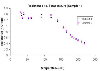
Resistance change of silicon coils in the cell as a function of temperature.
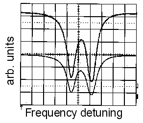
Cs optical absorption spectrum from a cell as it was heated with its in-situ heater to a temperature of about 75 °C. The N2 buffer gas pressure in the cell was nominally about 200 Torr.
Photograph of the cell heaters, taken under an optical microscope.
CAD layout of a large cell with in-situ heaters.
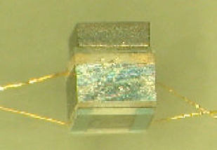
ITO heater assembly
Photograph of cell assembled with bonded ITO heaters
Heaters with reduced magnetic stray fields on ITO Thin films

(a) Photograph and (b) schematic side view of the ITO heater. Two glass substrates with patterned ITO are glued together with a nonconductive epoxy to make a heater with reduced magnetic fields. The lighter color lines in the heater are where ITO has been removed through laser patterning. After the ITO patterning, gold pads are deposited for wire bonding, and a 2 μm insulating layer of benzocyclobutene is deposited over the remaining exposed ITO so that electrical contact between the upper and lower ITO layers is made only through the gold pads. The large arrows show where current enters and exits the heater. The electrically conductive epoxy provides the connection between the upper and lower ITO.